Design overview
AXI memory map block appearance in a Simulink model,
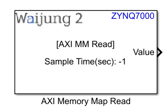
AXI memory map read block
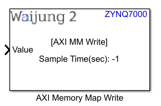
AXI memory map write block
AXI stream block mask overview,
AXI memory map read block
AXI memory map write block
AXI memory map block output interfaces,
AXI memory map read block
Name |
Type |
Range |
Description |
|||
Value |
|
Depends on the memory map
|
Read value from the given memory address registry |
AXI Stream block input interfaces,
AXI memory map read block
Name |
Type |
Range |
Description |
Base address |
uint32 |
Depends on the memory map
|
Specify the base address of registry to read. This port is enabled when the Configure base address and offset from input ports is enabled |
Offset |
uint32 |
Depends on the memory map |
Specify the offset value of registry address. This port is enabled when the Configure base address and offset from input ports and Enable offset are enabled.
If the Enable offset is enabled Memory address = Base address + Offset else Memory address = Base address |
AXI memory map write block
Name |
Type |
Range |
Description |
|||
Base address |
uint32 |
Depends on the memory map
|
Specify the base address of registry to write. This port is enabled when the Configure base address and offset from input ports is enabled |
|||
Offset |
uint32 |
Depends on the memory map |
Specify the offset value of registry address. This port is enabled when the Configure base address and offset from input ports and Enable offset are enabled.
If the Enable offset is enabled Memory address = Base address + Offset else Memory address = Base address |
|||
Value |
|
|
Specify value to write to the given memory address registry |
AXI memory map block behavior
AXI memory map block consists with two modes, read and write. This block is used to read value from the given memory registry address or write to the given memory registry address using memory map via AXI-4 interface.
AXI memory map block configuration
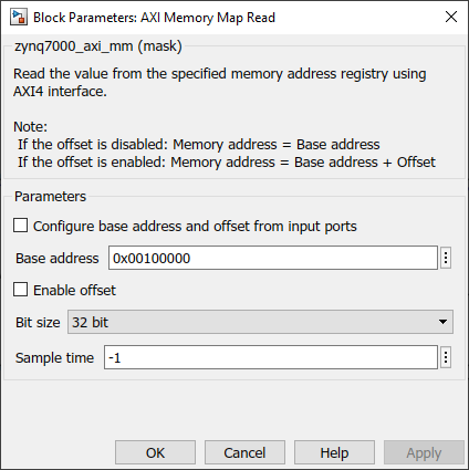
AXI memory map read block
Configuration Parameter |
Selectable Option/Value |
Default Value |
Description |
|||
Configure base address and offset from input ports |
|
off |
Configure the base address and the offset data from input ports |
|||
Base address |
|
0x00100000 |
Base address of the memory registry to read |
|||
Enable offset |
|
off |
Enable offset. |
|||
Offset |
|
0x0 |
Offset value which is use to add to the base address |
|||
Bit size |
|
32 bit |
Bit size of the read value from the given memory address |
|||
Sample time |
|
-1 |
Specify the sample time |
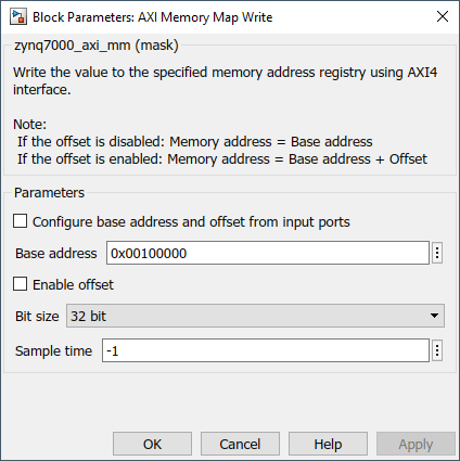
AXI memory map write block
Configuration Parameter |
Selectable Option/Value |
Default Value |
Description |
|||
Configure base address and offset from input ports |
|
off |
Configure the base address and the offset data from input ports |
|||
Base address |
|
0x00100000 |
Base address of the memory registry to write |
|||
Enable offset |
|
off |
Enable offset. |
|||
Offset |
|
0x0 |
Offset value which is use to add to the base address |
|||
Bit size |
|
32 bit |
Bit size of the write value to the given memory address |
|||
Sample time |
|
-1 |
Specify the sample time |
Typical application
Demo file is provided at:
[<waijung2 installation directory>\waijung2\targets\zynq7000\demo\axi_mm_demo]
To load the model file run the following commands in the Matlab Command Window:
•Demo 1: waijung2.openDemoInCurrentFolder('zynq7000', 'axi_mm_demo1')