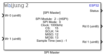
How this block appears in a Simulink model?
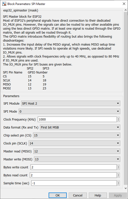
What can be configured?
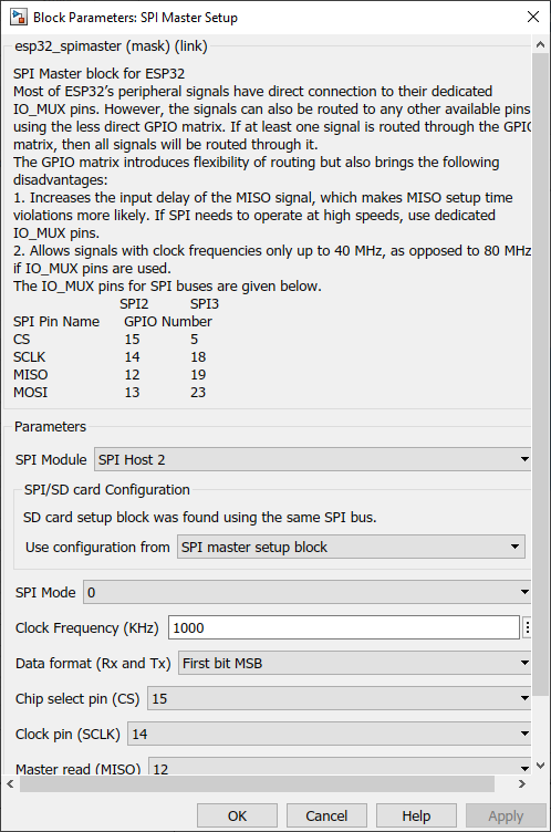
When the SD card block is not available in the same BUS
When the SD card block is available and use the same pins (BUS)
Configuration Parameter |
Selectable Option/Value |
Description |
SPI Module |
SPI Host 2----SPI Host 3 |
Specify SPI module for transmitting or receiving data. |
SPI Mode |
0--1--2--3 |
Select the SPI mode. |
Use configuration from |
SPI master setup block--SD card setup block |
If both SPI master setup and the SD card use the same bus(pins), select which configuration should be used to configure the SPI bus for both SPI master block and SD card. |
Clock Frequency (kHz) |
|
Transferring each byte takes eight times the clock period 8/fspi. If the clock frequency is too high, the use of some functions might be limited. |
Data format (Rx and Tx) |
First bit MSB--First bit LSB |
Select data format |
Chip select pin (CS) |
1 to 33 |
Select pin for CS |
Clock pin (SCLK) |
0 to 33 |
Select pin for SCLK |
Master read (MISO) |
Not used--0 to 33 |
Select pin for MISO |
Master write (MOSI) |
Not used--0 to 33 |
Select pin for MOSI |
Bytes write count |
|
Number of data bytes for write transaction (bytes sent via MOSI pin) |
Bytes read count |
|
Number of data bytes for read transaction (bytes sent via MISO pin) |
Sample time (sec) |
-1 (inherited) or specify |
Specify sample time for the block |
INPUT/ OUTPUT Port
Port Name |
Port Type |
Date Type |
Description |
Wr <x> |
Scaler |
UINT8 |
Input port to write the bytes. <x> is the write port number. |
Rd <x> |
Scaler |
UINT8 |
Output port to read the bytes. <x> is the read port number. |
Status |
Scaler |
UINT8 |
If error, status = -1 |
SPI pin name and function?
Pin name |
Alternative naming |
Function |
CS |
NSS, nCS |
Chip Select. Allows a Host to select individual Device(s) connected to the bus in order to send or receive data. |
SCLK |
SCK, CLK, CK |
Serial Clock. The oscillating signal generated by a Host keeps the transmission of data bits in sync. |
MOSI |
MDO, SDO, DO |
Master Out, Slave In, a.k.a. D. Data transmission from a Host to Device. |
MISO |
MDI, SDI, DI |
Master In, Slave Out, a.k.a. Q. Data transmission from a Device to Host. |
When using the ESP32 as SPI master, you can use any pins for the SCLK, MISO, MOSI, and CS signals, but using the following set of pins has minor advantages:
|
SPI2 |
SPI3 |
SPI Pin Name |
GPIO Number |
GPIO Number |
CS |
15 |
5 |
SCLK |
14 |
18 |
MISO |
12 |
19 |
MOSI |
13 |
23 |
If you use all of the pins for SPI2 or all of the pins for SPI3, using those pins is slightly faster, since the signals do not have to be routed through the GPIO matrix. This has the advantage of having a lower input delay (which is important at high speeds to avoid issues with MISO setup time) and that you can operate the SPI bus at 80 MHz (as opposed to 40 MHz with the GPIO matrix).
If you use ANY pin beside those listed above, ALL pins will be routed through the GPIO matrix – so use either all of these pins or ignore it altogether.
Note that some pins are input-only or reserved for special functions, so they may not be used for some or all of the SPI signals.
Demo
Target Demo file : esp32_spi_demo.slx
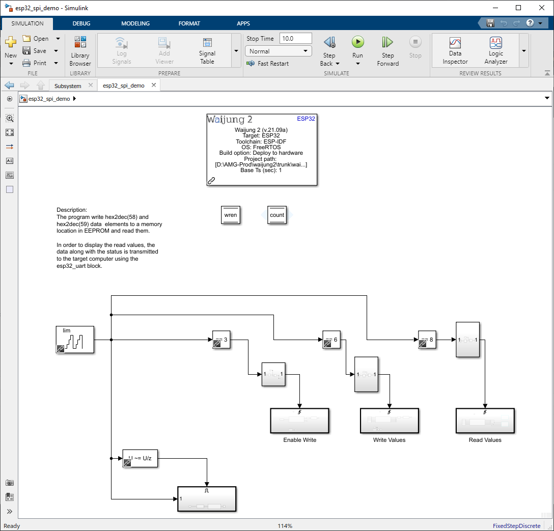
Subsystems in SPI demo
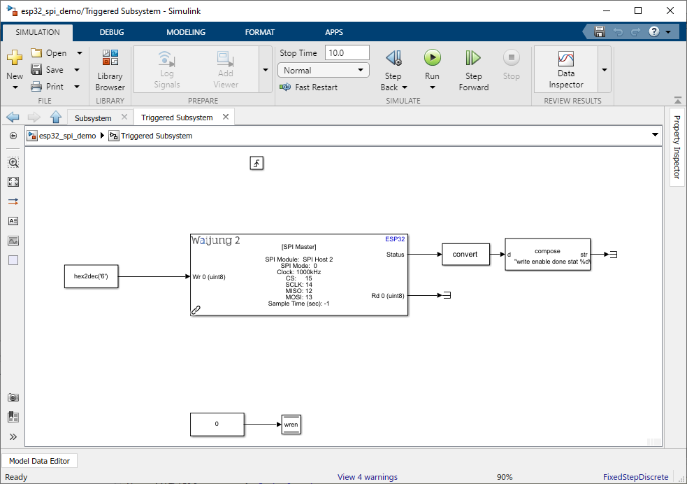
Enable Write Subsystem
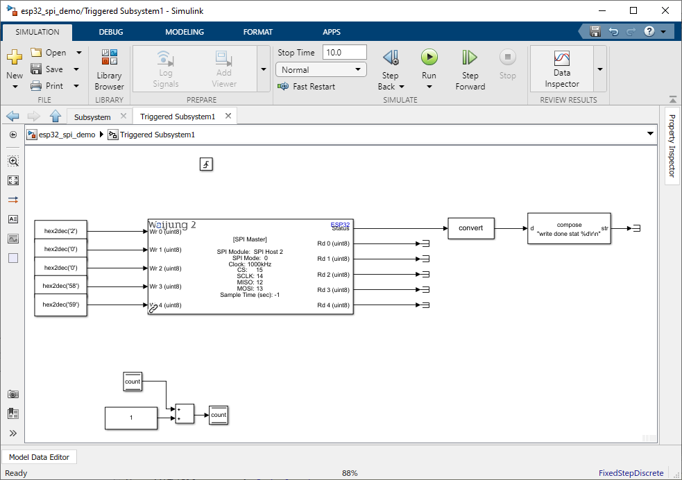
Write Values Subsystem
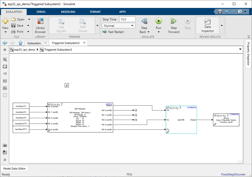
Read Values Subsystem
Description
This demo shows how to use the SPI master block and write and read data to an external SPI EEPROM module and print that data on the serial monitor.
Hardware Setup
1.ESP32 module
2.25AA512 512 Kbit SPI Bus Serial EEPROM
The CS pin (GPIO15), SCLK pin (GPIO14), MISO pin (GPIO12), and MOSI pin (GPIO13) should be correctly connected to the 25AA512 512 Kbit SPI Bus Serial EEPROM module.
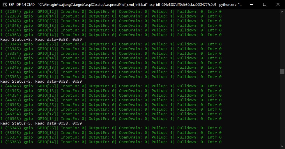
What should be happening?
After the hardware is set up and the SPI demo model is run on the ESP32, Use a serial monitor and select the corresponding COM port and the baud rate of 115200 to connect with ESP32. The written data to the SPI should be shown as in the following figure.